Home
Class E Overview and
Theory of Operation
Output Circuit Values & MOSFET ratings
High Power & Harmonic Reduction
Construction Overview
Simple 400 Watt
RF Amp for
80 meters
Using a lower power
transmitter as an
RF source (A to D converter)
Pulse Width Modulator and power supply
24 MOSFET RF Amplifier - Step by Step
Analog Modulator (Class H) and power supply
Overall Schematic of a complete modulator/power supply
![]()
.
Class H, High Efficiency Analog Modulator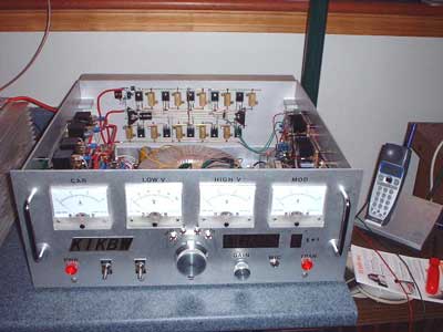
Combination class H modulator - power supply by Bob, K1KBW. This implementation uses 10 IRFP260N MOSFETs, 5 in the each leg of the modulator. The schematic shows 12 Devices (6 MOSFETs and 6 Bipolar Transistors), 6 in each leg. Up to 6 Devices may be used in each leg of the modulator. Schematic List:This is a class H, analog series modulator. This design is much more efficient than a standard class A series modulator, which would typically be around 30 or 35 percent efficient. The modulator has excellent audio performance, and is stable and easy to adjust. A system based loosely on this technology was used in the Harris MW1 Solid State 1KW Broadcast Transmitter. This technology is applicable to vacuum tube designs as well as other solid state designs. The idea behind class H, and a related class, class G, is to run the series modulator devices in the audio output at or near saturation. The voltage supplied to the near saturation devices is increased when greater output voltage is required. Otherwise, the when a lower output voltage is needed, the saturated device behaves like any other series modulator. In class G, the supply voltage supplied to the almost saturated output amplifier is stepped, and the number of power supply steps depends on the particular design. In class H, the supply voltage is adjusted linearly, rather than in a step function.
To The Right: Class H modulator-power supply built and designed by Steve, WA1QIX. The boards simplify the construction of the modulator. A complete board set is now available for the class H modulator and the Efficiency Meter / Overload Shutdown. Contact me if you're interested. More detailed Pictures of this class H modulator - power supply combination are Here. Note: there have been several revisions to the class H modulator since its first version. The current revision corrects several minor problems, and implements an overload shutdown function (requires external circuitry). A new PC board for this revision is forthcoming, however existing PC boards and implementations are still valid. |
.
MeteringThe schematics do not show meters. The following meters should be included:
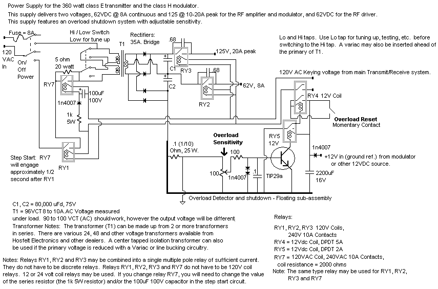
How the Class H Series Modulator WorksRefer to the Modulator Schematic and the Schematic of the Power Supply for a 350 to 450 watt transmitter... The modulator shown in the schematic can be used with any of the class E RF amplifiers shown here, operating at up to 450 watts of power. The principle is applicable to other transmitters and designs. The modulator is a source-follower series modulator which is operated nearly at saturation when the transmitter is producing only a carrier. This results in a low voltage drop across the primary modulator transistor (Q2), and consequently low dissipation and power loss in the device. The low-level drive circuitry "floats" with the output of the modulator. The op-amp U2, along with its related components and power supply is assembled onto a small piece of copper clad board, which is insulated from DC ground. Since the driver is floating along with the modulator output voltage, the input to the driver must be fed in such a way that the modulator output voltage does not affect the input. This is accomplished by using a differential amplifier as the first input amplifier, and referencing both the inverting and non-inverting inputs to dc-ground reference points. The voltage between the modulator output and DC ground will appear at both op-amp inputs equally, and will not appear at the output of the op-amp because there is no differential between the inputs caused by this voltage. Only a voltage difference between the inverting and non-inverting input of U2a will appear at the output. At carrier, the collector voltage of Q2 is fed through a diode from the carrier power supply. This supply is typically between 10 and 20 volts higher than the desired output voltage at carrier. Transistor Q1 is operated at cutoff when no modulation is present (carrier only). Since Q2 is a emitter-follower, the voltage appearing at the emitter of the transistor follows base voltage. The base voltage is set such that the output of Q2 is approximately 46-47 volts - about 15-16 volts less than the power supply voltage of 62V. The base voltage is supplied to Q2 through the driver MOSFET, through a 4.7K resistor, fed from a Zener diode, which drops the power supply voltage by 12V. So, the voltage measured at the base of Q2 with respect to ground will be around 46 volts. The threshold voltage of the driver MOSFET is approximately 4 volts (the gate voltage needs to be about 4 volts higher than the source voltage in order for the MOSFET to conduct). So, the source voltage from the driver MOSFET will be 4 volts lower than the gate voltage (which is around 50V.), resulting in between 45 and 46 volts from the source of the driver to the base of Q2. Q2 will exhibit approximately .7 volts of drop. With this arrangement, the carrier level is set by the power supply voltage, since the DC output voltage of the modulator will directly track the power supply voltage. No other adjustments are necessary to set the carrier voltage. The gate of Q1 is connected directly to the output of op-amp U2c through a 12V Zener diode. The DC output voltage of op-amp U2c is 0V DC, as measured between the floating sub-assembly and the op-amp output. The floating sub-assembly is connected to the source of Q2 (which is the output point of the modulator). At carrier, the source of Q2 and the modulator output is sitting at approximately 46 V above DC ground. So, the gate of Q1 will be approximately 12V higher, or around 58V. DC. During the positive peak modulation cycle, the output of U2b and U2c will increase. This will drive the gate of the Q2 driver higher (Q3), driving the base of Q2 higher. Since the emitter voltage of Q2 will follow the base voltage, the voltage drop across Q2 will decrease, and the Q2 emitter voltage, and the modulator output voltage will increase. At the same time, the voltage fed to the gate of Q1 is also increasing. When the gate voltage of Q1 reaches approximately 66 volts with respect to DC ground, Q1 will begin to conduct. So, the voltage drop across Q2 will drop by approximately 8V before Q1 begins to conduct. Since the voltage no-signal voltage drop across Q2 is approximately 16 volts, no distortion will result, because Q1 will begin to supply more voltage to Q2 before Q2 saturates. At all times, Q2 is the primary modulating device. Q1 simply supplies additional drain voltage to Q2 as the output voltage increases. It is important to note that during positive peaks, the 200V 10A diode between the collector of Q2 and the carrier power supply is back biased. No current flows from the carrier power supply at this time, and the supply is effectively switched out of the circuit. The gate voltage of Q1 is fed through a diode, and therefore the gate will only be driven when gate voltage, as referenced to ground exceeds the source voltage. Otherwise, the diode is back-biased. During the negative portion of the modulating waveform, the voltage fed to the bases of Q2 drops, and Q2 acts as a normal emitter follower series modulator. Voltage is fed to Q2 from the carrier power supply through the 200V 10A series diode. The diode feeding the gate of Q1 is back-biased, Q1 is completely cut off and effectively out of the circuit. I have also designed a very simple mic preamp/equalizer/compressor (peak limiter) to go with the class H modulator. The schematic is Here. The Power SupplySchematic of the Power Supply for the class H modulator |
